8-VSB Transport Clock Synthesis
Interested in how to generate a 19.39265846 MHz clock? Perhaps more applicable would be that 38.78531692 MHz SMPTE-310M clock. 27 MHz appears to be a pretty common frequency in video applications, so we'll run with that. Assume you have a 27 MHz crystal or can somehow generate a 27 MHz clock.
Recall that the bit rate came from the following equation in the A/53-2:
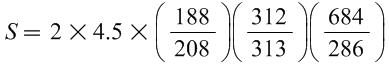
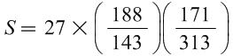
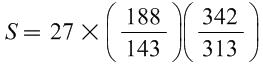
We want a factor that we can multiply by 27 to obtain 19.39265846, so after factoring out a 27 from the numerator and simplifying the rest of the terms we get:
Of course, if a SMPTE-310M transmitter is your end goal, you have to multiply by 2:
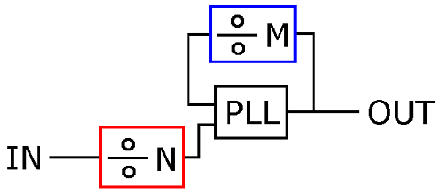
PLL Clock Multiplication
To multiply a clock or any frequency, you need a PLL. A PLL is a feedback circuit, and it tries to make the signal in its feedback pin equal in frequency and phase to the signal in its reference pin.
What if you stuck a clock divider in the feedback path? The PLL output would then have to be faster because the divider will generate a slower signal that has to be matched to the reference.
Consider a reference of 10 MHz and a clock divider of 5. At the feedback pin the PLL wants a 10 MHz signal, so the output would have to be 50 MHz. Thus dropping in a divide by 5 counter causes the PLL to multiply the reference signal by 5!
That's all well and good, but we can also divide the input such that a slower signal appears at the reference pin. Now what? Suppose we divide the input by 3. The overall effect is a fractional multiplication by 5/3. The figure below illustrates the typical M/N PLL multiplier configuration.
So is it a simple matter of putting a divide by 64296 block in the feedback path and a divide by 44759 block in the input path? In theory, yes! In reality, getting it to work will be difficult.
Just what is the frequency of the clock at the reference pin then? You have to divide 27 MHz by 44759, leaving you with a grand total of about 603.23 Hz. These days most PLL's accept an input reference in the MHz or even hundreds of MHz range. The best case scenario you can get away with is a two-PLL configuration.
Altera FPGA Implementation
PLL's integrated into FPGA's are nice because they come with internal clock dividers, eliminating the need to go out to FPGA logic fabric. Unfortunately, you can't currently get a Xilinx FPGA to synthesize this kind of clock. Xilinx's Virtex-5 new PLL can only multiply by up to 64 and divide by up to 52 [PDF]. Altera's Cyclone III and Stratix III FPGA's, on the other hand, support factors up to 512!
You can try to factor the numerator and denominator integers and use more PLL's, but 313 is a prime number. Kaboom.
So what, you might say. Just create a clock divider using a counter in the Virtex-5's (massive amounts of) logic fabric, buffer the divided clock, and then send it into the PLL. But remember that most PLL's don't go into the kHz range of inputs, and that includes the Virtex-5's PLL.
With a III-series FPGA, create two PLL's in Quartus MegaWizard with the appropriate counter values, connect the output of one to the input of the other, and connect the 27 MHz clock to the PLL with the free input (although, where else would you connect it?).
But I can't get my hands on those sweet, sweet Cyclone/Stratix III's
If you're a Xilinx fanboy or fangirl, or just have to get on with older Altera parts, you're going to have to go off-chip and get two external PLL's capable of locking on inputs in the kHz range. Two possible parts are the 662 and MK9173, both made by IDT. The 662 has no loop filter, requiring you to supply two capacitors and a resistor, so the MK9173 Genlock PLL is a much more convenient solution.
The strategy remains the same: chain the PLL's together. This time, the counters are going into FPGA fabric. What this means is the following:
- 27 MHz drives a counter. Make it drive the divide by 143 counter.
- Route the divide by 143 output to the reference pin of PLL 1.
- Route PLL 1's output back to the FPGA and through a clock buffer. Now you have a clock, say
PLL_1_CLK. PLL_1_CLKdrives two counters, one that divides by 313, and another that divides by 188.- The divide by 188 output goes out to the feedback pin of PLL 1, while the divide by 313 output goes to the reference pin of PLL 2.
- Route PLL 2's output back to the FPGA and through a clock buffer. This will be the 38.78531692 MHz clock signal. Call it something short.
- In addition to driving a FIFO, the 38.78531692 MHz clock has to drive a divide by 342 counter.
- Route the divide by 342 counter output to the feedback pin of PLL 2.
Got all that? Good. Will it work? I'm just a n00b, so all bets are off.
Why should you divide by 143 first? Because the resulting clock frequency is 188.811 kHz, which is higher than the 86.262 kHz you'd get from dividing by 313 first. It's not much, but the higher the better. Just because a PLL can lock to a slower reference doesn't mean you should push it.
Confused? Have Some RTL!
- clk_syn.vhd — clock dividers implemented as counters
It may or may not compile, but it should be a reasonable teaching aid. Knock yourself out.
Equation images were generated using the LaTeX to Bitmap feature at TeX2MathML!
|